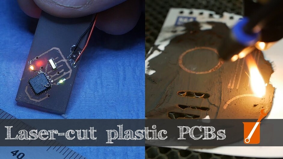
This came up in my video feed. Seemed interesting. I haven’t done boards, so I don’t know if anyone else would need to do this…
Interesting, for sure. I used to visit contract manufacturers for KVM switches & got to see a lot of PCBA & SMT operations. Big differences between high volume & low volume operations. PCBs usually multiple layers (4-8 common, even 12) and often traces imbedded within layers, as well as the thru hole VIAs. The ability to 3D print them is huge (as well as flexible PCBs) for smaller devices, shapes & even wearable electronics. For low volume, laser makes sense vs. cost of jigs and such for cutting & drilling boards. For flat traditional PCBs, pending the size of the board, the individual PCB is left as part of a large panel w/ edges for handling thru all the prep & assembly processes, and once the panel of multiple boards is completed (or assembled, A in PCBA), the individuals are snapped apart. And lasers are used to add manufacturing info & SNs to the PCBs, and likely already widely used for cutting–pending the interaction of the laser vs. the layers & traces vs. mechanical stresses other cutting, the board house uses the most cost efficient method, which could vary widely pending board type & design & scale of manufacturing (1000 or millions).
I watched the whole video. He is amazing, as always. Definitely some understanding of chemistry is helpful.
It’s kind of slim on the laser side of things, as in not going into a whole lot of detail. More on the chemistry side of things. He’s got a 60 watt, but it doesn’t seem to need lots of power.
PLA is not suitable for this method. He doesn’t mention any other FDM materials that I noted.
This topic was automatically closed after 32 days. New replies are no longer allowed.
