Not sure it would suffice for that. Sure it would be in the same place software-wise, but how do you make sure the hardware (material to be lasered) is in the exact same place (i.e. shape centered 2 inches from the top and 3 inches from the left. It would be there in the software, but how do you precisely place the wood so it shows up in that spot)
Unless the grid lines itself up to the piece versus the bed, but I don’t think that is what @karaelena was intending.
I used the grid to assist with lining up the design to an existing feature on the workpiece. The best thing to do for work piece repeatability is using something (like magnets) on the work surface and using that as a hard stop.
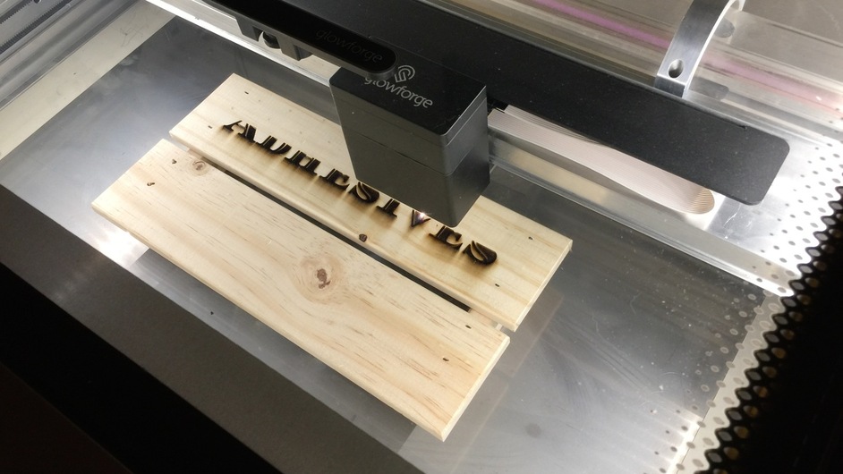
My main thing was engraving something on something that was a irregular shape and not square.
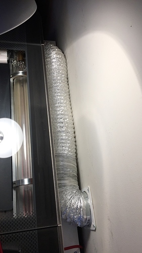
was very helpful to me, as the space I will have behind the Glowforge and the wall behind it (leading up to the window for venting) is pretty tight. This relieved my mind, a bit. Thank you!
This is great! Can you break these out into separate posts? I know we sometimes get sloppy about new posts for new topics, but there’s so much interest in your work it’d do a disservice to leave these prints at the end of a long thread.
Someone on the forums posted an up close picture of trying to cut glass at full power and multiple passes.
The result was more fracturing than etching/cutting.
With masking or cermark/thermark, the energy from the beam is concentrated at the masking versus being reflected/diverted (especially as the material of glass either fractures or melts/liquifies). Now I want to say this mainly applies to lower powered lasers, but not playing with large units, I am uncertain.
The focus from the laser head is not referring to the focal point of the beam, but more of the auto focusing of the Glowforge.
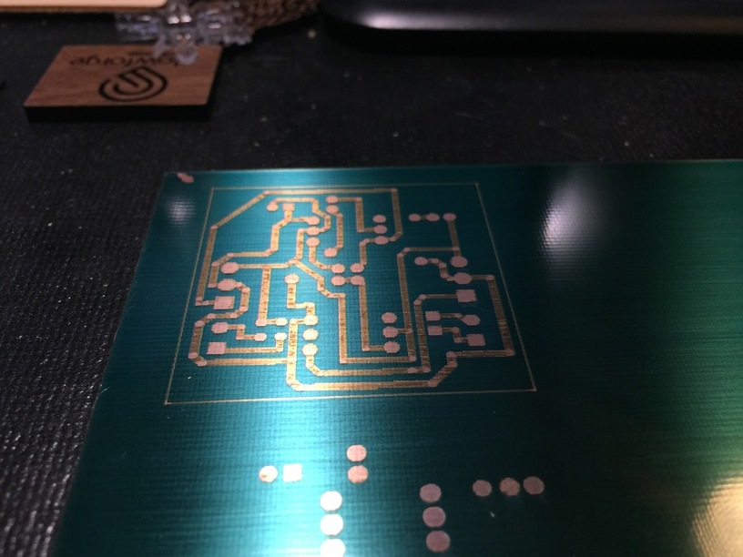
From what I have referenced from making ones own circuit boards after using software like Eagle PCB design by Cadsoft ,to name one, it helps with layout and modificatin of the board then can be imported in to a laser system to remove the conductive material to build and test prototype boards or maybe now make replacement boards in simple devices. Food for thought maybe but since it the conductive material is most often a copper coat either a cermark or paper mask would be recommended. I have also learned that the active ingredient in Cermark is the same as CRC moly drylube spray and if I recall DM-90 for etching stainless steel.
If you already etch your own PCBs (probably in very small quantity for prototypes or small-scale production) then being able to zap away the resist removes a bunch of steps from the workflow. Usually you make a mask, align that with the PCB (sometimes transfer it physically), expose the masked PCB to UV(?) light to fix the resist, then wash away the unfixed resist and etch. This effectively reduces the process to zap and etch.
It would be nice if a gf could also drill, but nuh-uh. (Although now I wonder: if you made pads-to-be-drilled with little holes through the copper in the center, could you punch a laser though that if your alignment were good enough? And would it be worth the trouble?)