Even if it’s not graphene, the fact that it’s conductive is great news. I take it that the laptop tape isn’t conductive before treatment… Just checking lol.
Is there anything the Glowforge’s laser can shoot through without cutting? I was thinking you could sandwich the laptop between two layers of ‘laser permeable’ material, laser your circuit design and this might give you a more robust end result.
It could be graphite, but I was following the procedure dictated in the Nature article above. Also, technically, graphene is just a single layer of graphite. So, since this process makes almost a graphene foam, I guess you could call it graphite if you want.
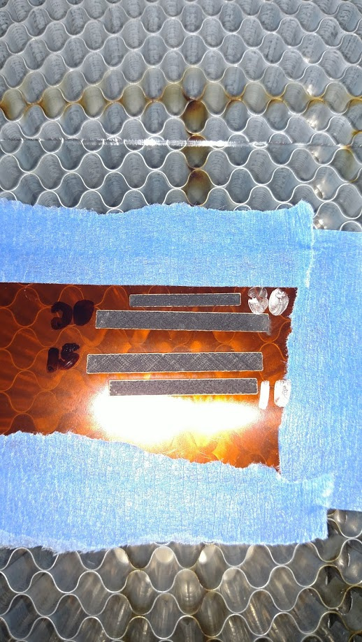
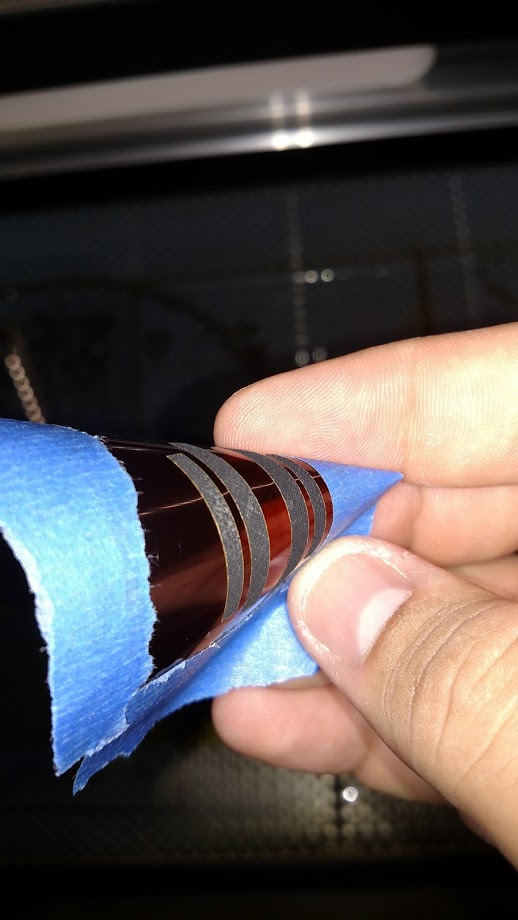
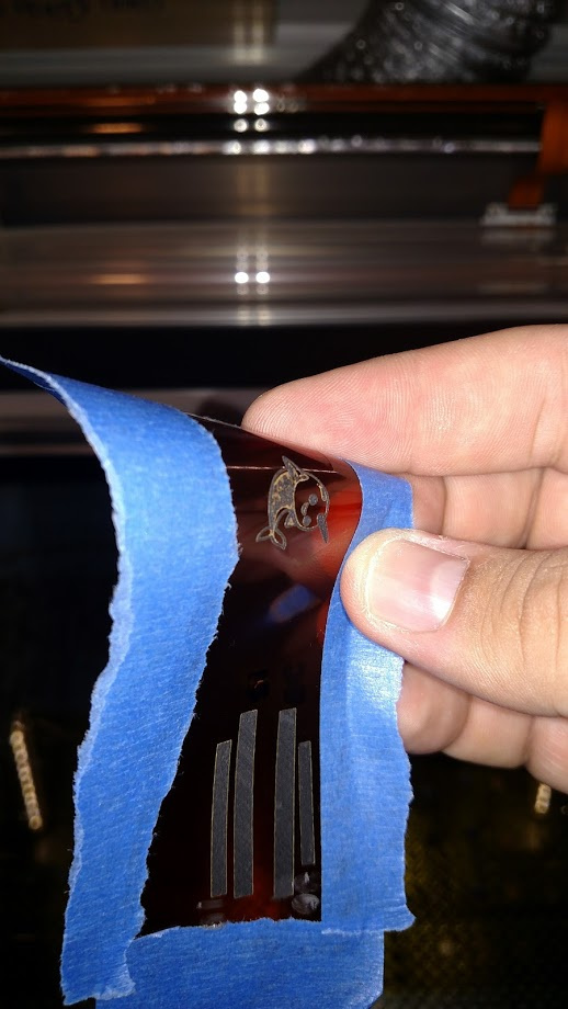
The resistances were around 15-50Ohms, but they increased as I was probing; I believe that’s due to the LIG flaking. I believe this is due to me using a thinner Kapton tape with silicone adhesive on it instead of a thicker Kapton sheet with no adhesive, similar to what was done in both papers above. I have some scrape thicker sheets I was going to play around with later.
It the thicker sheet works, then it will be very stable without needing any additional material. They have demonstrated being able to bend LIG without breaking it.
Interesting. The nature of graphine suggests it’s an extremely (one atom) thin layer you’re creating. With the thicker sheet are they simply converting the top layer of Kapton into Graphene and leaving the subsurface as Kaptop? If so, then it’d be pretty strong.
Any ideas on how to attach components to such a material?
From my understanding, this is similar to a pyrolysis process. You are essentially burning away the Nitrogen and Oxygen and leaving the Carbon behind. The way they describe it is a “porous graphene films with three-dimensional networks”.
As for connecting to it, they used silver ink. I was just relying on the “foam” it generated to connect and flow over the wires. There connection was probably better than mine.
Unfortunately, I don’t have the equipment at home to verify that it is graphene. I’m working on getting funding through work to do more testing on this, otherwise I’m limited to just resistance measurements. These seem in line with what the paper is suggesting they should be, so I’m going to move forward with the assumption that it is LIG.
I would suggest reading the paper I linked above. This is generating a porous graphene, not a flat sheet.
@joe Have you considered multiple layers of kapton or other backing material to hold it together? My brother is taking his advanced chemistry class to Argonne’s Advanced Photon Source (APS) where they use coherent x-rays to probe detailed atomic positions. I thought an experiment like yours might be appropriate for them to study. What do you think? They are looking for ideas.
BTW, I am also interested in solving the flexibility problem so that I can use the graphene as an electrode in a flexible gel pack battery I am studying. If my memory is correct, we might be able to use amperometric methods to estimate the surface area of the graphene.
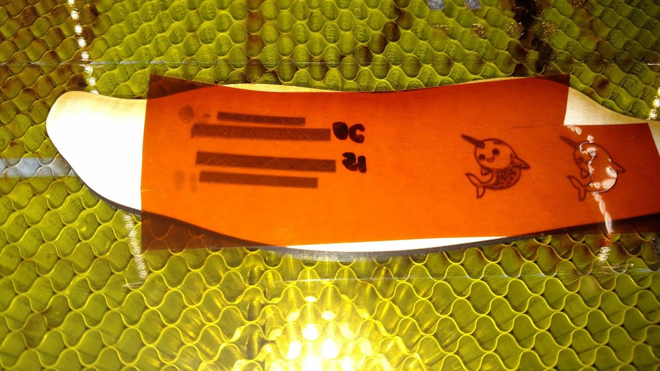
The strips I made above that lit the LED were done with 2 pieces of Kapton, stuck together back to back. They did not penetrate the second layer. From what I can tell, it appears that all my tests did not go through the silicone adhesive on the back of the Kapton.
I have a thicker scrap of Kapton without any adhesivie. I’ll try running some tests tomorrow. (D&D tonight )
Having it tested at APS would be AWESOME!!! Do you want me to send you some samples, or do you want to make it yourself?
This is very interesting. is there any chance that any treatment on the graphene to make it solder-able and become a flexible PCB or a capacitance touch pad?

 )
)